
The Catalyst of the Nanotechnology Era: The Microscope
Nanotechnology is made possible because of the instruments used to see things on the nanoscale. The invention of these happened years before the term nanotechnology was coined, but their invention is of course still worth mentioning. They form the basis of nanotechnology today. Here we will see some of the key microscopes scientists and engineers use to work at the nanoscale. They allow us to be able to see at the nanoscale, to characterise with nanoscale materials and surfaces and to move things around on surfaces in order to create devices.
Scanning Electron Microscope (1931)
An electron microscope depends on electrons rather than light to view an object. . The electrons interact with the atoms that make up the sample producing signals that contain information about the sample's surface topography, composition, and other properties such as electrical conductivity. Electrons are speeded up in a vacuum until their wavelength is extremely short, only one hundred-thousandth that of white light. Electron microscopes make it possible to view objects as small as the diameter of an atomErnst Ruska co-invented the electron microscope for which he won the Nobel Prize in Physics in 1986.
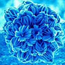
‘’Flowers’’ of silicon carbide and Gallium, 3D Nanostructure. Image courtesy of Ghim Wei Ho and Prof. Mark Welland, Nanostructure centre, University of Cambridge/NSF
|
The scanning electron microscope remains a crucial instrument in nanotechnology. Scanning electron microscopy (SEM) can be exploited for nanomaterials characterization but also integrated with new technologies for in-situ nanomaterials engineering and manipulation. SEM can be used for nanomaterials imaging, X-ray microanalysis, high-resolution SEM, low kV SEM, cryo-SEM, as well as new techniques such as electron back scatter diffraction (EBSD) and scanning transmission electron microscopy (STEM). Fabrication techniques integrated with SEM, such as e-beam nanolithography, nanomanipulation, and focused ion beam nanofabrication, are major new dimensions for SEM application. Application areas include the study of nanoparticles, nanowires and nanotubes, three-dimensional nanostructures, quantum dots, magnetic nanomaterials, photonic structures, and bio-inspired nanomaterials. [4]
|
Scanning Tunneling Microscope (1981)
The STM works by scanning a very sharp metal wire tip over a surface. By bringing the tip very close to the surface, and by applying an electrical voltage to the tip or sample, we can image the surface at an extremely small scale – down to resolving individual atoms. The STM is based on several principles. One is the quantum mechanical effect of tunneling. It is this effect that allows us to “see” the surface. Another principle is the piezoelectric effect. It is this effect that allows us to precisely scan the tip with angstrom-level control. Lastly, a feedback loop is required, which monitors the tunneling current and coordinates the current and the positioning of the tip.[5]
The images taken with these microscopes look like tumulose alien landscapes—and researchers learned how to rearrange those landscapes, once they discovered that the scanning tunneling microscope could also be used to pick up, move, and precisely place atoms, one at a time. The first dramatic demonstration of this power came in 1990 when a team of IBM physicists revealed that they had, the year before, spelled out the letters “IBM” using 35 individual atoms of xenon.
The images taken with these microscopes look like tumulose alien landscapes—and researchers learned how to rearrange those landscapes, once they discovered that the scanning tunneling microscope could also be used to pick up, move, and precisely place atoms, one at a time. The first dramatic demonstration of this power came in 1990 when a team of IBM physicists revealed that they had, the year before, spelled out the letters “IBM” using 35 individual atoms of xenon.
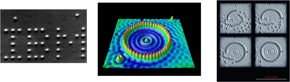
Image 1: In November 1989, Don Eigler of IBM and his team used a custom-built microscope to spell out the letters IBM with 35 xenon atoms. This unprecedented ability to manipulate individual atoms signaled a quantum leap forward in nanoscience experimentation and heralded in the age of nanotechnology. Image 2 is an artificial corral structure created from 48 iron atoms on copper electron waves. Eigler and colleagues created this structure in 1993 by using the tip of a low-temperature scanning tunneling microscope to position iron atoms on a copper surface, creating an electron-trapping barrier. This was the first successful attempt at manipulating individual atoms and led to the development of new techniques for nanoscale construction. Image 3 shows four different stages of the atom movement for the creation of the corral in image one.
Atomic Force Microscope (1986)
1986 - Gerd Binnig, Quate, and Gerber invent the Atomic Force Microscope (AFM).It Can measure surfaces in a very accurate way using a probe tip mounted on a cantilever beam like a diving board. The position of the tip is monitored with a laser beam which is refelected off the cantilever on to a detector. As the tips scan back and fourth it moves up and down with the hills and valleys of the surface, which deflects the laser beam up and down. The information is recorded on a computer. From the information collected we can understand information about the surface. It's possible to scan any surface with an AFM and at such high resolution amazing things can be seen . The AFM probe can also examine the friction of a surface. Different regions of a surface have different frictional properties as the tip scans along. The instrument can feel forces from a physical object but it can also feel forces of electric charge. The image on the left shows four silicon pads on a surface. The yellow pad looks higher than the rest but it's not. It's a representation of the distribution of electrical charge on a surface. The more elevated pads have the most charge.[6]
Single-walled carbon nanotubes have been attached to the tip of an AFM probe to make the tip “sharper”. This allows much higher resolution imaging of the surface under investigation; a single atom has been imaged on a surface using nanotube-enhanced AFM probes. Also, the flexibility of the nanotube prevents damage to the sample surface and the probe tip if the probe tip happens to “crash” into the surface. [7] |
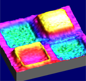
Electric force microscopy image of charge spreading on small silicon pads on silicon dioxide.
Olivia Castellini and Mark Eriksson, University of Wisconsin - Madison
|
Field Emission Microscope (1936)
Erwin Wilhelm Müller invented the field emission microscope. This is a device in which electrons liberated by field emission are accelerated toward a fluorescent screen to form a magnified image of the emitting surface. FEM was one of the first surface analysis instruments that approached near-atomic resolution.
Field Ion Microscope (1951)
Erwin Wilhelm Müller invents the field ion microscope and is the first to see atoms. FIM is an analytical technique used in materials science. The field ion microscope is a type of microscope that can be used to image the arrangement of atoms at the surface of a sharp metal tip. It was the first technique by which individual atoms could be spatially resolved. On October 11, 1955, Muller & Bahadur (Pennsylvania State University) observed individual tungsten (W) atoms on the surface of a sharply pointed W tip by cooling it to 78 K and employing helium as the imaging gas. Muller & Bahadur were the first persons to observe individual atoms directly; to do so, they used an FIM, which Muller had invented in 1951.[8]
Transmission Electron Microscope (1931)
Transmission electron microscopy (TEM) is a powerful tool for analysis of structure and devices with nano-meter scale dimensions. Transmission electron microscopes utilize very thin (0.5 µm or less) samples illuminated by an electron beam. Images are recorded by detecting the electrons that pass though the sample to a system of electromagnetic lenses which focus and enlarge the image on a fluorescent screen, photographic film or digital camera. Magnifications beyond 1,000,000x are attainable with a transmission electron microscope. The first TEM was built by Max Knoll and Ernst Ruska in 1931, with this group developing the first TEM with resolving power greater than that of light in 1933 and the first commercial TEM in 1939. [9]
